
Friday, August 5, 2016
silicon on insulator CMOS
the picture speaks about the difference in topology of the device. The device at the top is a normal CMOS that the diffusion is implanted in the substrate but the one at the bottom, the substrate is insulated with an oxide region from the part of silicon that would construct the device channel. The benefits are: lower leakage, lower substrate noise to the channel, no body connection is required, device can operate lower than VDD, etc.

Monday, August 1, 2016
Logical Effort: design logics in CMOS
so far found the following chapters of "Logical Efforts" by Sutherland, Sproull, and Harris:
Chapter 1: The Method of Logical Effort
Chapter 4: Calculating the Logical Effort of Gates
Chapter 10: Circuit Families
and this presentation slide by Harris.
Chapter 1: The Method of Logical Effort
Chapter 4: Calculating the Logical Effort of Gates
Chapter 10: Circuit Families
and this presentation slide by Harris.
Friday, July 29, 2016
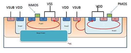
Deep N Well to isolate nmos devices
deep N wells are used in customized analog layouts where (a) nmos base voltage is not connected to ground (e.g. to avoid body effect), or (b) noise reduction is important. In the latter case, by putting nmos's P well in an n-well/ ring, P substrate noise cannot go to nmos device pins. More details in this post from Planet Analog.

Wednesday, July 27, 2016
Thursday, June 2, 2016
Transforms and Applications Handbook
"Transforms and Applications Handbook" is a handbook of transform functions. I came across this reference in the Hilbert transform introduction by Frank Kschischang.
Wednesday, March 30, 2016
Current Mode Logic Active Inductor Load
Active inductor load can be designed by applying a negative voltage feedback from drain of an active current load to the gate of the active load. The feedback has a time constant that depends on the size of gate resistor and Cgs of the active load. Overall, feedback makes the load to behave like an inductor where $L=\frac{R_g C_{gs}}{g_m}$. For more details refer to page 68 of this Master's thesis. The following image is also captured from the thesis.


Tuesday, March 29, 2016
Spectre Simulation (Fundamental)
"Simulation of Analog and Mixed-Signal Circuits by Ken Kundert" slides are a quick review of the book, "The Designer's Guide to SPICE and Spectre". The book goes through the details of spice simulation and explains the trad-offs.
CMOS chopper amplifier to reduce 1/f noise
The paper reviews CMOS chopper amplifier theory and actual circuit. The theory is simple: modulate the input signal to F_chopper where 1/f noise is not significant, amplify the modulated signal. and finally demodulate and reconstruct low pass signal at the output. Also, found this work interesting: using CMOS devices in lateral bipolar mode to decrease 1/f noise (see figure 14).
Subscribe to:
Posts (Atom)